Building DMF Surfaces
The PurpleDrop itself consists of hardware and software for driving the high-voltage signals to electrodes, sensing capacitance, and controlling peripherals, such as temperature control. This section is not about that. This section is about how to build the DMF “chip”, or “cartridge”: the surface on which the drops move. The drop surface is a separable module, plugged into the PurpleDrop via two board-to-board connectors.
There are different techniques for building drop surfaces. Typically, drops are actuated under a glass “top-plate”, but it is also possible to leave the top plate off and move drops on an open surface. The surface is typically disposable, as it has a limited operational lifetime. Here is a generic representation of a DMF surface:

Here’s a typical, generic DMF surface diagram. Different designs use varying materials, and deposition methods for the various layers. The top plate is, in some cases, optional.
Here, we document how we typically build surfaces to be used with the PurpleDrop, and provide some existing designs. The PurpleDrop can drive most types of DMF surfaces fine, as long as you have a suitable adapter to get the electrical signals from the purpledrop connectors to your electrodes! Our approach to building surfaces is intended to make it as easy as possible to build them in small quantities with the minimum of special lab equipment. They are based around printed circuit boards, off-the-shelf components, and spin-coated coatings.
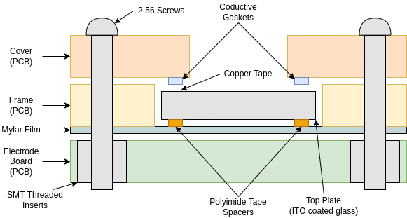
Cross section of typical PurpleDrop electrode board stackup. Three different PCBs are used to create the electrodes, hold the dielectric film/top plate in place, and provide electrical connection to the top plate ITO coating.

Examples of Electrode board (MISL v6.1), dielectric frame, and cover (from pd-frame-50x75)
Building the Electrode Board PCB
For PurpleDrop, we pattern electrodes on PCBs for easy manufacturability. We have a few different designs, and instructions for creating custom designs.
Building the Dielectric Layer
For the dielectric layer, we use 6um thick Mylar film stretched over a PCB frame. The mylar is then coated with a hydrophobic layer via spin-coating. This method helps to create a flat surface for drops to move on, masking the relatively large height of the copper layer on typical PCBs. The frame can also be used to locate the top plate relative to the electrodes.
For instructions on how to assemble a dielectric film, see Mylar Film Carrier Assembly.
Here are some existing PCB designs for the carriers:
Building the Top Plate
The top plate is made from ITO-coated glass. We add a piece of copper tape (with conductive adhesive) to one edge to allow connection to the ITO layer from the opposite side, add kapton tape spacers to maintain the appropriate gap between the top plate and the dielectric film, and coat the ITO layer with a hydrophobic coating.
For instructions on assembling the top plate, see Top Plate Preparation.
Holding it Together (the Cover)
Finally, the third PCB used in the assembly is the “cover”. It is screwed down over the top plate, and serves both to hold the top plate in place, and to provide electrical contact to the top plate. The cover typically has one connection point for a wire, and connects to the top plate by conductive, compressible foam gaskets.
Designs for covers are included in the repositories linked above, under “Building the Dielectric Layer”.