Designing a Custom Electrode Board
One of the main advantages of using a PCB as a DMF substrate is that custom boards can be built quite cheaply and quickly by the many PCB manufacturers that cater to low-volume prototype production. Designing an electrode board is very similar to any other PCB design, and can be done in the same electrical CAD software. At MISL, our electrode boards are typically designed in KiCad and we have created some python tools to help with electrode pad design and layout.
PCB Design Rules
Feature size
Typically, we have used copper-to-copper clearance of 0.004” (4 mils) between pads. While the most basic and cheapest PCB processes are sometimes limited to 6 mil spacing, 4 mil spacing is still readily available for modest increase in cost.
Layers
Most electrode boards can be done in two layers, with the electrodes on the top layer, and the connectors with connecting traces on the bottom layer. For some boards – e.g. the v4.1 electrode board – we have used 4 layers to make room for heaters on the bottom and to provide internal planes for better heat conduction.
Vias
The electrodes must be connected by placing vias inside each one. It is possible using “via-in-pad” processes provided by many PCB manufacturers to fill these holes with epoxy, and plate over them for a continuous pad with no hole. This process may double the cost of the boards, but may be necessary in certain cases, such as when creating many vias underneath a single electrode to improve heat conduction to the bottom layer. When only one via is placed in each electrode however, it is generally fine to leave the small hole in the middle of the electrode. The dielectric film stretched over the electrodes covers the hole and provides a flat surface for drops to move on, and the loss of electrode area is so small as to have a seemingly negligible effect on drop movement.
For electrode vias, a drill size of 0.2mm is typically used.

Examples of electrodes with standard open vias (left), and filled vias (right).
Thickness
The most common PCB thickness is 1.6mm, and this is a good size for an electrode board. Thinner board have proved to be too flexible, and this can lead to variations in the gap size between the electrodes and top plate over the working area of the board.
Connector Pinouts
One challenging – and error-prone – task is determining which electrode is connected to which high voltage output pin. For most electrodes, it does not make any difference which pin it is connected to, however there is one important exception to this: the top plate must be connected to pin 97, as this pin is wired to the current sensing circuit.
The easiest way to get the pinout correct is to use this KiCad template project as a starting point for your design. It includes the two connectors, placed at the appropriate distance apart, and with net labels already assigned according to the software pin labelings.

Top-down view of PurpleDrop electrode board connectors, showing pins numbered according to software pin numbering.
Mounting Holes
Most PurpleDrop electrode boards use mounting holes with soldered on nuts in the corners for securing the dielectric film to the board with 2-56 screws.
Keystone 4929 inserts can be soldered into 3.7mm plated holes.
Other Concerns
Copper Pours for Planarity
It’s important to have good planarity over the active area of the board in order to maintain equal distance between the dielectric film and the top plate. To that end, it is recommended that you pour copper over the entire board, and leave it uncovered by soldermask. This means that the spacers of the top plate will rest directly on copper, which will be at the same height as the copper electrodes.
This copper pour can be left unconnected, or it can be connected to an electrode pin, which will allow it to be used as guard rail for straying drops. For example, if you place a copper pour around a reservoir the capacitance measurement for that pin can be used to detect if the drop on the reservoir has moved off onto the guard; you can then pull it back by briefly activating the appropriate reservoir electrode(s).
Placing fiducials in copper wells
Fiducials may be placed in silkscreen on top of soldermask. It is recommended to use a dark soldermask under white silkscreen. Because the soldermask + silkscreen height is substantial and comparable to the 0.035mm height of 1oz copper, you should place the fiducials inside a cutout in the copper pour, so that they do not sit up above the plane of the copper and cause tenting of the dielectric film around the fiducial.
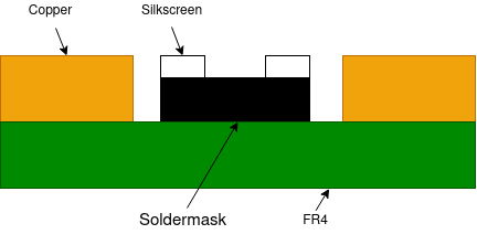
Cross section of soldermask and silkscreen fiducial placed inside a square hole in the copper to avoid a bump in surface height.
Electrode Layout Process
For a step-by-step tutorial on how to create electrode footprints, import these to kicad, layout the board using python scripts, and create fiducial footprints, see the Basic electrode board design tutorial in the dmfwizard documentation.